Gw12 prototypes
From Glacsweb Wiki
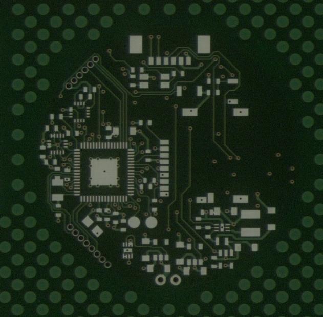
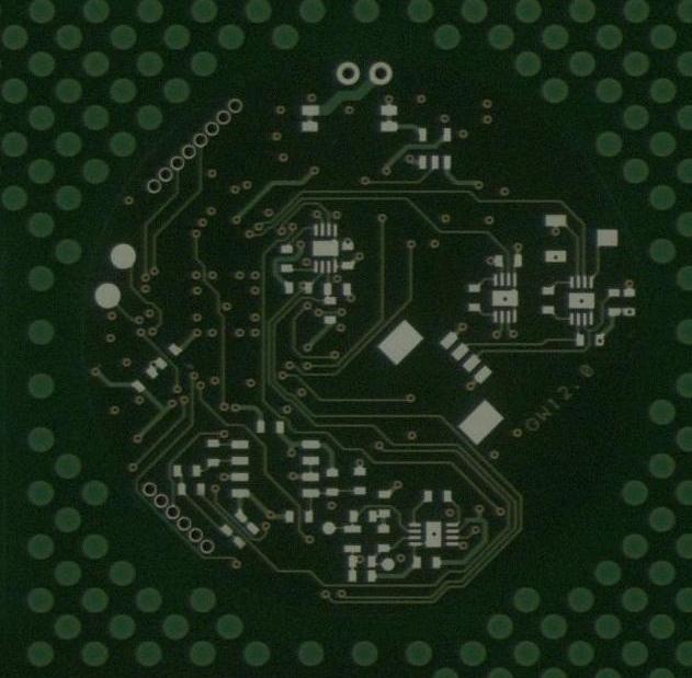
First home-built probes look like:
Contents
Connectors
Top White Connector
From right to left.
| Pin | Name | Details |
|---|---|---|
| 1 | VDD_SENSORS | Sensors 3.3V Supply |
| 2 | GND | 6 |
| 3 | Pressure+ | 9 |
| 4 | Pressure- | 12 |
| 5 | Resistance | 15 |
| 6 | Resistance_Offset | 15 |
Top Left Through-hole Connector
Pins are numbered from Left to Right
| Pin | Name | Details |
|---|---|---|
| 1 | GND | Conencted to common ground |
| 2 | VDD | Connected to MCU 3.3V |
| 3 | !RESET | Inverting Reset: High=Active, Low=Reset |
| 4 | SWO | Single Wire Output for Advanced Debugging |
| 5 | SWCLK | Single Wire Clock |
| 6 | SWDIO | Single Wire Debug Input/Output |
Bottom Left Through-hole Connector
Pins are numbered from bottom right to upper left. There are a couple of problems here, as all the signals are 3.3V Logic, while the radio is driven with a 5V Supply. Must investigate whether all these lines are neccessary
| Pin | Name | Details |
|---|---|---|
| 1 | GND | Blahde blah |
| 2 | VDD_RADIO | 5V Radio Supply Signal |
| 3 | RADIO_RESET | |
| 4 | RADIO_TX | 12 |
| 5 | RADIO_CTS | 15 |
| 6 | RADIO_RX | 15 |
| 7 | RADIO_SETUP | 15 |
| 8 | RADIO_WAKE_DIR | 15 |
IC's counter-clockwise from top left
- HMC5883 Compass
- MMA 8450 Accelerometer
- EFM32G230F128
- LTC2935 Voltage Supervisor
- LP5951 3.3V LDO (MCU Voltage Plane)
- LP5951 3.3V LDO (Sensors enable Sensors Plane)
- TPSsomething-something Boost Reg
- REG113 LDO smoothing reg
Other devices on board:
- microsd card slot
- 3 colour led
- 2x Tactile Buttons
IC's around board
- 3x INA333 Instrumentation Amps
- Analog switch (bottom)
- OPA2333 Operational Amplifiers
- Power Switch
.jpg/1024px-Gw12prototop_(Medium).jpg)
_(2).jpg/1024px-Gw12protobot_(Medium)_(2).jpg)

